Deep know-how.
Broad capability.
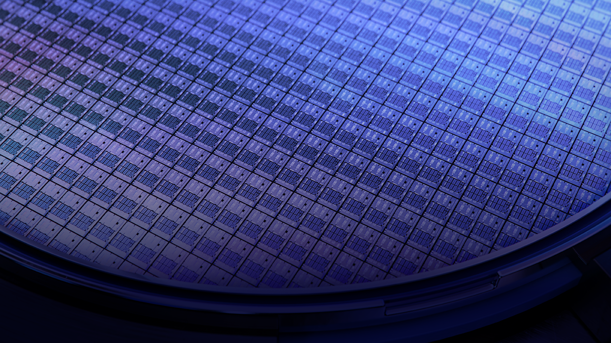
We design and build photonic devices and systems. Our integrated approach combines research, intellectual property, materials expertise, process engineering and manufacturing. One facility. Every stage connected.
Plessey operates across two distinct application areas: microLED displays for AR and VR, optical computing, and optical interconnects. Each demands specialist expertise. Each is advancing at Plessey simultaneously, under one roof.

MicroLED panels use microscopic light-emitting diodes as individual pixels.
Each pixel generates its own light. No backlight, no colour filters, just direct emission at unprecedented brightness and efficiency.
Plessey designs and manufactures microLED panels optimised for AR and VR applications. This is the most demanding display environment that exists: near-eye, always-on, performance-critical. We engineer for it precisely.
Key capabilities
5 million nits achievable. Outdoor-readable, HDR-capable. Light output that conventional displays cannot match.
Lower power consumption per lumen. Battery life extended. Thermal management simplified.
Individual pixel control. Extremely high contrast ratios. Uncompromising image quality across the full brightness range.
Inorganic LEDs resist degradation. No burn-in. Stable performance over operational lifetime.
Smaller pixel pitch enables higher resolution in smaller areas. Critical for near-eye displays and compact devices.
Applications
Augmented reality and mixed reality require displays that are small, bright and efficient. MicroLED delivers all three. Head-up displays for automotive and aerospace benefit from brightness and reliability. Consumer electronics gain efficiency and image quality.
Our microLED technology is designed for people, engineered to scale.

Data centres are not limited only by the speed of their processors.
The connections between them – chip-to-chip, card-to-card, rack-to-rack – consume around 25% of total system energy when electrically connected. At the scale of modern AI infrastructure, that is an enormous and growing problem.
Plessey designs and manufactures photonic devices for optical interconnects. By replacing electrical signals with light across these connections, data moves faster and with lower latency, at a fraction of the energy cost.
Plessey’s optical interconnect technology cuts the interconnect energy burden by a factor of 10. At higher data rates. With lower latency.
Why it matters
Optical interconnects are an essential part of future AI infrastructure. They depend on precise, high-performance photonic devices, engineered to specification.
Where computation density matters, photonics delivers.
Our approach

Integrated operation
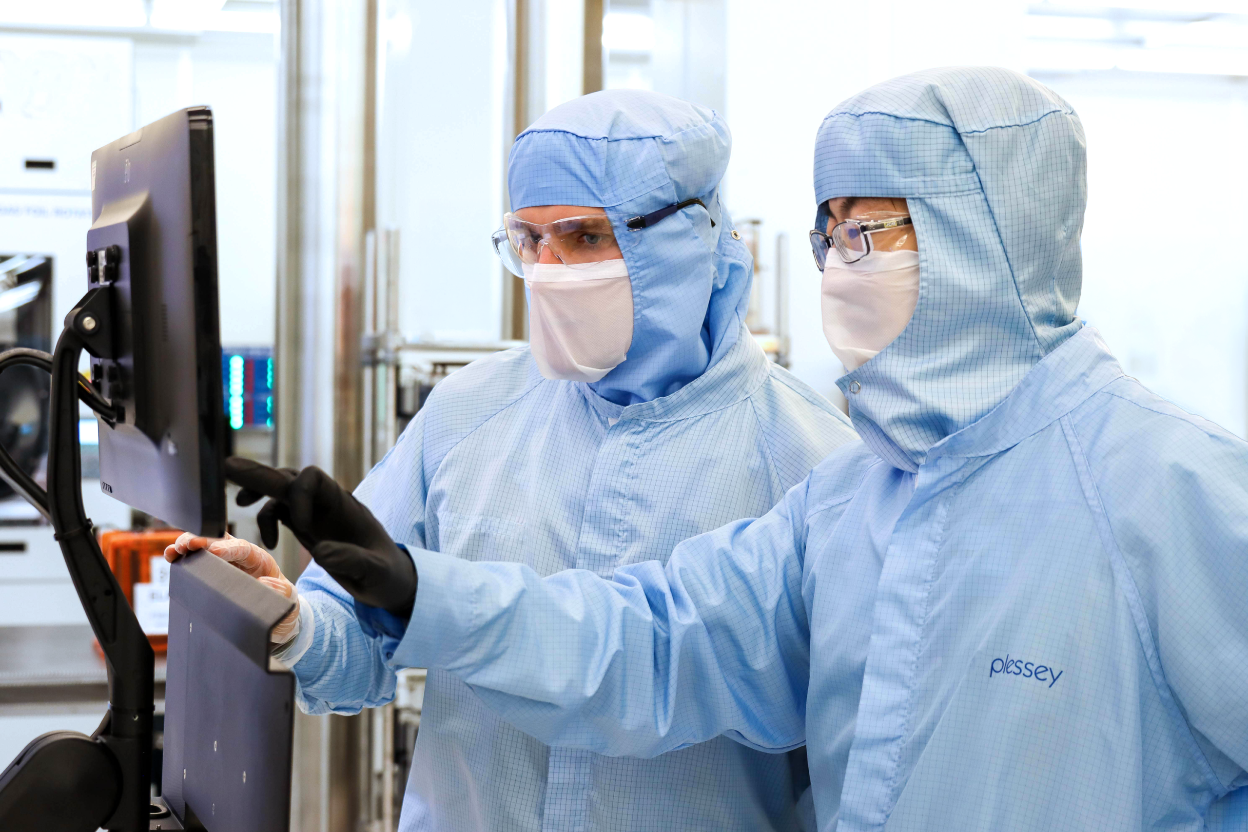
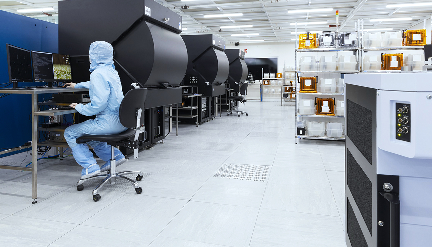
Research, intellectual property, materials science, process engineering and manufacturing: all under one roof. Our Plymouth facility enables rapid development cycles and maintains quality control across every stage.
When discovery happens in the laboratory, it is tested in the cleanroom within days. When process engineers identify improvements, manufacturing implements them immediately. Integration accelerates innovation.
Quality standards
ISO 9001:2015 certified. Our quality management system ensures consistent results, documented processes and continuous improvement. Standards maintained, performance verified, commitments met.
Seventy years of innovation
From early semiconductor development through modern photonics, we have been advancing technologies for more than seven decades. The expertise runs deep. The capability runs broad.