TEst

Why monolithic integration wins the race to build microLED displays

We’ve become used to very high resolution displays on our smartphones, with some offering pixel densities of up to 400dpi – arguably greater than most human eyes can resolve. These displays are almost always built using LCDs, and represent the current state of the art for a technology that has been in development for over half a century.

As we move to a more intimate interaction with technology and the virtual world it brings us, through body-worn electronics such as smart watches, fitness trackers, virtual-reality helmets, and augmented-reality glasses, the display technology we use will have to change. LCDs, which use changing crystal alignment to block or allow the passage of photons from a backlight, must give way to emissive technologies that turn electrons into photons directly.

There are a couple of key contenders for this replacement technology, including OLEDs and microLEDs, that is arrays of small LEDs mounted at tight pitches on some sort of backplane. OLEDs have had some traction in the market, but are between 100 and 1000 times less bright than LEDs for the same electrical input. This really matters in applications such as head-up displays, where, because of the difficulty of coupling the light emitter to an optical waveguide, very little of the light produced actually reaches the user’s eye.

MicroLEDs rely on the electro-optical characteristics of III-V materials such as gallium nitride (GaN) to directly emit photons. Some companies create microLED arrays by mounting discrete GaN LEDs on sapphire substrates, at pitches that begin at 50um and may have to shrink down to as little as 10um for very small or very high-resolution displays. To build a full colour HD panel this way, with a resolution of 1920 x 1080 pixels in three colours, would mean accurately placing more than 6.2 million LEDs with positional accuracies of at least +/-10um.

This kind of individual device placement will never make economic sense, if it means tying up an expensive pick and place machine for days or weeks simply to produce a single display for a $500 pair of AR glasses. To tackle this, manufacturers have experimented with techniques such as transferring multiple microLEDs from the wafer they were made on using an adhesive film as a transport. Work is also going on to build massively parallel pick and place machines, which can pick up an array of LEDs from the source wafer and then place them simultaneously on their target substrate. In both cases, there are multiple issues with maintaining positional and alignment accuracy across all the placement sites.

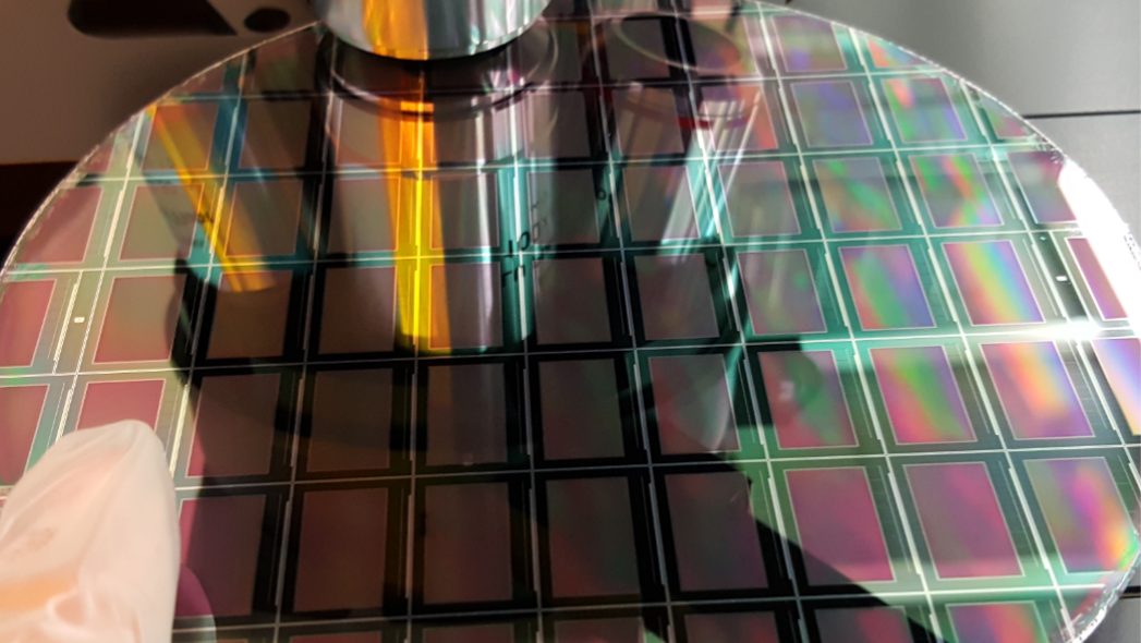
In a sense, the development of microLED arrays is a classic Moore’s Law story, in which monolithic integration is obviously the right ultimate answer, but it takes many intermediate steps to achieve it. However, Plessey has developed their proprietary monolithic approach to building GaN microLEDs directly on a CMOS silicon substrate, so that placement and alignment accuracy are now controlled by lithography, a very well understood process in the semiconductor industry.

Plessey showcased a World’s first prototype earlier this year at Display Week in San Jose. The microLED display features an array of 1920×1080 (FHD) current-driven monochrome pixels on a pitch of just 8 microns. Each display requires more than two million individual electrical bonds to connect the microLED pixels to the controlling backplane. The Jasper Display Corp eSP70 silicon patented backplane provides independent 10-bit single colour control of each pixel.


Silicon substrates have greater thermal conductivity than sapphire, allowing the microLEDs to be driven harder before their output becomes thermally limited. A CMOS silicon substrate also makes it very easy to build the addressing and switching matrix for controlling the microLEDs, and to integrate other supporting circuitry, perhaps even graphics processing units, on the same wafer. The Plessey GaN-on-silicon process already scales to 200mm wafers, and can be scaled further, enabling economies of scale in manufacturing that will not apply to working on smaller sapphire substrates.


Most current microLED arrays use three devices to produce the R, G, B outputs necessary for a full colour display. But recent research suggests that it may be possible to build more sophisticated microLEDs that can produce R, G, B and intermediate colours (through mixing) from one device. Once again, the monolithic integration predicted and championed by Moore’s Law wins.


Plymouth manufacturer disrupting the global display market with its proprietary GaN-on-Silicon microLED display technology

Plessey, an embedded technologies developer located on the edge of Plymouth, UK, is disrupting the global display market with a new generation of Augmented Reality (AR) devices and display solutions using their unique and IP protected MOCVD based GaN-on-Silicon (GaN-on-Si) monolithic microLED display technology.

Up until 2017, the business model was focussed on high-powered solid-state lighting, horticultural lighting and healthcare/ safety sensors sectors. This changed when senior management took a risk to pivot to the research and development of microLED’s. This advanced and cutting-edge technology is the first new display technology to be commercialized in over a decade and will replace existing LCD and OLED technologies used in an array of applications from HDTVs to smartphones, smart watches, Head up displays (HUDs), and AR headsets.

A microLED display has many advantages such as high brightness, ultra-low power consumption, fast response time, very high contrast rate, wide colour gamut, long lifetime, environmental stability, high resolution, the option of flexible backplanes and integration of sensors in the display. Its main challenges are manufacturing complexity and yield issues, all of which Plessey are addressing, through its innovative and cutting-edge technology.

Consumer electronics and television manufacturers such as Samsung, LG, Apple etc. are all looking to create products using microLED technology, which could dramatically improve the functionality, durability and longevity of their products. MicroLED forecasting report by n-tech Research projects the overall market opportunities for microLED technology to grow from $0.5B to $22.4B by 2024.

Plessey has had a highly successful year with the development of its microLED technology, and has received recognition from the electronics and display industry globally with successful exhibition shows, technical speaking opportunities, and receiving multiple awards including being named as a CES 2019 Innovation Awards honoree in the ‘Embedded Technologies’ category, in addition to having a double-win at the Electronics Industry Awards for ‘Display Product of the Year’ and the ‘Embedded Solution Product of the Year’.

Chris Bailey, Plessey’s Financial Director & Controller, said:

“Plessey is continually striving to innovate and deliver manufacturing excellence, and this past year saw a record result in sales following three years of continual growth. The recent technology breakthroughs such as the development of the native green light and achieving the world’s first GaN-on-Silicon monolithic full HD microLED bonded displays, would not be possible without the continual investments and highly-skilled workforce based at our Plymouth facility.”

A recent investment includes the refurbishment of an underutilised area, which has been completely transformed into a modern mixed work and leisure space. The new space, designed by AMH Projects, features break-out areas with comfortable velvet sofas, private booths and a fully functioning kitchen; offering a space for both employees and external visitors to use and enjoy.

As the microLED technology drives forward, there is a phased plan to modernise other key areas at Plessey. Supporting this, the company will invest heavily in recruitment, with the aim to increase the current headcount of 140 to an estimated 170 employees by 2020. The company will also undergo a comprehensive corporate rebranding, including a new company logo.

Sam Langridge, Plessey’s Marketing Manager said:

“The rebranding reflects both the evolution of the company as well as its vision for the future. The branding will further enable the company to stand out in the emerging microLED market whilst giving a clear outlook to our customers and stakeholders. A new milestone within our organisation has been reached and the rebrand is a testament to the confidence we have in the innovative and cutting-edge technology we are developing”

The space was officially opened with a ribbon cutting ceremony on Tuesday 10th September 2019. Attendees included local dignitaries from Plymouth City Council, Plymouth University, Plymouth Manufacturing Group, DIT and local manufacturing businesses to help celebrate the exciting new space, and to hear about Plessey’s latest technology breakthroughs, investments and future plans.

About Plessey

Plessey is an award-winning provider of full-field emissive microLED displays that combine very high-density RGB pixel arrays with high-performance CMOS backplanes to produce very high-brightness, low-power and high-frame-rate image sources for head-mounted displays (HMDs), and augmented reality (AR) and virtual reality (VR) systems. Plessey operates leading-edge 150mm and 200mm wafer processing facilities to undertake design, test and assembly of LED products, and a comprehensive suite of photonic characterization and applications laboratories. For more information, visit Plessey’s website, Twitter, Facebook and LinkedIn pages. 

Media Relations Contacts:

Sam Langridge, Marketing Manager | sam.langridge@plesseysemi.com | +44 1752 693 000

Paige Lee, Marketing Executive | paige.lee@plesseysemi.com | +44 1752 693 000